|
データシートサーチシステム |
|
|
データシートサーチシステム |
|
MCP6V06T データシート(PDF) 22 Page - Microchip Technology |
|
|
|||||||||||||||||||||||||||||
MCP6V06T データシート(HTML) 22 Page - Microchip Technology |
|
|
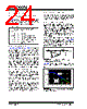
22 / 44 page  MCP6V06/7/8 DS22093B-page 22 © 2008 Microchip Technology Inc. 4.1.2 AUTO-ZEROING ACTION Figure 4-2 shows the connections between amplifiers during the Normal Mode of operation ( φ1). The hold capacitor (CH) corrects the Null Amplifier’s input offset. Since the Null Amplifier has very high gain, it dominates the signal seen by the Main Amplifier. This greatly reduces the impact of the Main Amplifier’s input offset voltage on overall performance. Essentially, the Null Amplifier and Main Amplifier behave as a regular op amp with very high gain (AOL) and very low offset voltage (VOS). FIGURE 4-2: Normal Mode of Operation ( φ 1); Equivalent Amplifier Diagram. Figure 4-3 shows the connections between amplifiers during the Auto-zeroing Mode of operation ( φ2). The signal goes directly through the Main Amplifier, and the flywheel capacitor (CFW) maintains a constant correc- tion on the Main Amplifier’s offset. The Null Amplifier uses its own high open loop gain to drive the voltage across CH to the point where its input offset voltage is almost zero. Because the principal input is connected to VIN+, the auto-zeroing action corrects the offset at the current common mode input voltage (VCM) and supply voltage (VDD). This makes the DC CMRR and PSRR very high also. Since these corrections happen every 50 µs, or so, we also minimize slow errors, including offset drift with temperature ( ΔVOS/ΔTA), 1/f noise, and input offset aging. FIGURE 4-3: Auto-zeroing Mode of Operation ( φ 2); Equivalent Diagram. 4.1.3 INTERMODULATION DISTORTION (IMD) The MCP6V06/7/8 op amps will show intermodulation distortion (IMD), products when an AC signal is present. The signal and clock can be decomposed into sine wave tones (Fourier series components). These tones interact with the auto-zeroing circuitry’s non-linear response to produce IMD tones at sum and difference frequencies. IMD distortion tones are generated about all of the square wave clock’s harmonics. See Figure 2-37 and Figure 2-38. VIN+ VIN– Main Output VOUT VREF Amp. Buffer NC Null Amp. CH CFW VIN+ VIN– Main Output VOUT VREF Amp. Buffer NC Null Amp. CH CFW |
|
リンク URL |
| ALLDATASHEETはお客様のビジネスに役立ちますか? [ DONATE ] |
Alldatasheetは | 広告 | お問い合わせ | プライバシーポリシー | データシートへのリンク | リンク交換 | メーカーリスト All Rights Reserved©Alldatasheet.com |
| Russian : Alldatasheetru.com | Korean : Alldatasheet.co.kr | Spanish : Alldatasheet.es | French : Alldatasheet.fr | Italian : Alldatasheetit.com Portuguese : Alldatasheetpt.com | Polish : Alldatasheet.pl | Vietnamese : Alldatasheet.vn Indian : Alldatasheet.in | Mexican : Alldatasheet.com.mx | British : Alldatasheet.co.uk | New Zealand : Alldatasheet.co.nz |
|
Family Site : ic2ic.com |
icmetro.com |
 Japanese ▼
 English
 Chinese
 German
 Japanese
 Russian
 Korean
 Spanish
 French
 Italian
 Portuguese
 Polish
 Vietnamese
 Indian
 Mexican
 British
 New Zealand