|
データシートサーチシステム |
|
|
データシートサーチシステム |
|
ISL73847SEHDEMO2Z データシート(PDF) 29 Page - Renesas Technology Corp |
|
|
|||||||||||||||||||||||||||||
ISL73847SEHDEMO2Z データシート(HTML) 29 Page - Renesas Technology Corp |
|
|
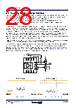
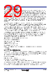
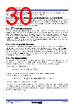
29 / 40 page  R34DS0017EU0104 Rev.1.04 Page 29 Jan 31, 2025 ISL73041SEH Datasheet 6.11 Gate Driver Outputs The ISL73041SEH features independent source and sink driver outputs for the rise and fall time control. The upper gate driver is the Upper Gate High (UGH) and Upper Gate Low (UGL) pins. The lower gate driver is the Lower Gate High (LGH) and Lower Gate Low (LGL) pin. A series diode is needed on drivers without separate source and sink pins to achieve independent turn-on/off control. This issue can be problematic for GaN FETs as the diode's voltage drop from driver output to the FET gate impacts the FET ON-resistance. If no turn-on or turn-off time reduction is needed, Renesas recommends inserting a 0Ω resistor anyway. In practical layout, the Printed Circuit Board (PCB) trace length connecting the driver output to the FET gate has a parasitic inductance. Combined with the parasitic capacitance of the FET gate, this forms a resonant loop that can cause excessive ringing in the gate drive waveforms during turn-on and turn-off. The ringing overshoot may be large enough to damage a GaN FET gate in a poor layout. A small amount of resistance may be required to dampen the overshoot. The UGx and LGx output high peak drive currents that turn on and off the FET quickly for high-frequency applications need to minimize switching losses. The high-side driver provides up to 2A source and 4A sink peak drive current. The low-side source and sink driver provides up to 4A source and 8A sink peak drive current. There is a 1kΩ passive pull-down resistor on UGL to PHS and a 500Ω passive pull-down resistor on LGL to PGND. These passive pull-down resistors prevent charge build-up on the FET gate-source capacitance when the ISL73041SEH driver is not biased. Otherwise, both half-bridge FETs can accumulate enough Vgs from leakage current or stray noise at the capacitive high impedance gate to turn on and cause shoot-through. In normal operation, driver outputs respond to PWM input commands. Under disabled or fault conditions, the driver outputs do not respond to PWM input, and the driver outputs are in either an active off (the UGL and LGL sink drivers are on) or passive off (1kΩ pull down on UGL to PHS and 500Ω pull down on LGL to PGND) condition. Below is a list of ISL73041SEH states where the driver outputs do not respond to PWM input commands and their associated active or passive states. Note: A passive off condition supersedes the active off condition. ▪ EN pin low (driver disabled): Passive Off ▪ VDD, AVCC or PVCC UVLO: Passive Off ▪ PWM = Mid level: Active Off ▪ FLT externally driven low: Active Off ▪ Over-Temperature Fault: Active Off ▪ BOOT UVLO: Passive off only at the high-side driver. The low-side driver is still active to PWM input commands. 6.12 FLT Pin Fault Indication The ISL73041SEH includes several fault protections to prevent the operation of the half-bridge driver in a faulted condition. The FLT pin is an indicator of its fault status. The FLT pin is a dual-use open-drain output with external input control. Connect a pull-up resistor from the FLT pin to AVCC. The typical value is 10kΩ. FLT internally pulls low to indicate a fault condition when one of the following occurs: ▪ EN = 0 (driver disabled), ▪ VDD, AVCC or PVCC in UVLO, or ▪ ISL73041SEH is in an over-temperature fault condition. Under these fault conditions, the driver outputs do not respond to PWM inputs. You can also use the ISL73041SEH FLT pin for external control input in fault broadcasting applications where all driver FLT pins are connected. If one driver or a controller enters a fault condition that pulls its FLT pin low, all other ISL73041SEH drivers are disabled to prevent operation when the system detects a fault condition. |
|
リンク URL |
| ALLDATASHEETはお客様のビジネスに役立ちますか? [ DONATE ] |
Alldatasheetは | 広告 | お問い合わせ | プライバシーポリシー | データシートへのリンク | リンク交換 | メーカーリスト All Rights Reserved©Alldatasheet.com |
| Russian : Alldatasheetru.com | Korean : Alldatasheet.co.kr | Spanish : Alldatasheet.es | French : Alldatasheet.fr | Italian : Alldatasheetit.com Portuguese : Alldatasheetpt.com | Polish : Alldatasheet.pl | Vietnamese : Alldatasheet.vn Indian : Alldatasheet.in | Mexican : Alldatasheet.com.mx | British : Alldatasheet.co.uk | New Zealand : Alldatasheet.co.nz |
|
Family Site : ic2ic.com |
icmetro.com |
 Japanese ▼
 English
 Chinese
 German
 Japanese
 Russian
 Korean
 Spanish
 French
 Italian
 Portuguese
 Polish
 Vietnamese
 Indian
 Mexican
 British
 New Zealand