|
データシートサーチシステム |
|
|
データシートサーチシステム |
|
ISL73847SEHDEMO2Z データシート(PDF) 30 Page - Renesas Technology Corp |
|
|
|||||||||||||||||||||||||||||
ISL73847SEHDEMO2Z データシート(HTML) 30 Page - Renesas Technology Corp |
|
|
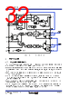
30 / 40 page  R34DS0017EU0104 Rev.1.04 Page 30 Jan 31, 2025 ISL73041SEH Datasheet For SEE mitigation, Renesas recommends using a 10pF or larger capacitor on the FLT pin to SGND. This capacitor prevents false toggling of the FLT pin due to SEE transients. 6.13 FLT pin Usage with ISL73847SEH and other ISL73041SEH drivers The ISL73041SEH FLT pin works with the ISL73847SEH PWM controller as a system-ready status to initiate soft- start (not in fault) or shutdown (fault encountered) in operation. The ISL73847SEH is a 2-phase controller, so both the FLT pin on the ISL73041SEH and the FLT pin on the ISL73847SEH are tied with a single pull-up resistor to either the AVCC on ISL73041SEH or VCC on ISL73847SEH. 6.14 FLT as Pseudo Enable Pin The EN pin enables the bandgap before powering up the PVCC LDO and finally enabling the driver outputs. The propagation delay time from the EN rising edge to the driver output's enable is 95µs typical. Alternatively, for faster enable time in applications not using the ISL73847SEH PWM controller, an open-drain NMOS FET can be connected to the FLT pin to operate as a faster enable/disable pin. When the gate voltage is logic high, the FLT pin is low, and the driver is disabled. When the gate voltage is logic low, the pull-up resistor on the FLT pin pulls the FLT high. The FLT high or low to the driver output's response propagation delay is 100ns typical. When using the FLT pin as the driver enable pin, connect EN to VDD. 6.15 Over-Temperature Protection The ISL73041SEH integrates an Over-Temperature Protection (OTP) circuit. When the junction temperature reaches 160°C typical, the OTP threshold is triggered. In an over-temperature fault condition, the driver stops responding to PWM inputs while the UGL and LGL sink outputs are active to disable the half-bridge. The FLT pin pulls low to indicate a fault. The PVCC LDO remains enabled during an over-temperature fault condition. When the junction temperature falls below 145°C typical, the OTP condition clears. The driver automatically resumes normal operation, and the FLT pin is released. 6.16 VDD Supply Current The VDD supply current of ISL73041SEH divides between static bias current and dynamic operating current. The static bias current includes the current needed to bias the dead time delay circuit. The dynamic operating current consists of the operating frequency on PWM, the duty cycle, and the capacitive load of the GaN FET. The static bias current is approximately: where VREF = 1.2V; RDU and RDL are the resistors (in kΩ) used for the dead-time delay. The dynamic operating current is approximately: The dynamic I_VDD current vs fSW is found in Figure 47. The dynamic current from the capacitor load is I = C × V × F, where C is the equivalent capacitive load of the GaN FET gate-source capacitance, V is the operating PVCC voltage, and F is the switching frequency (fSW). Determine C by QGS/V, where QGS is the total gate charge specified in the GaN FET datasheet. Remember to sum up the low and high sides of GaN FET QGS. (EQ. 5) (EQ. 6) I_VDD (static) 4.5mA 3 VREF RDU ----------------- 3 VREF RDL ----------------- ++ = I_VDD (dynamic) I_VDD fSW I_VDD (capacitor load) I_VDD (duty cycle) ++ = |
|
リンク URL |
| ALLDATASHEETはお客様のビジネスに役立ちますか? [ DONATE ] |
Alldatasheetは | 広告 | お問い合わせ | プライバシーポリシー | データシートへのリンク | リンク交換 | メーカーリスト All Rights Reserved©Alldatasheet.com |
| Russian : Alldatasheetru.com | Korean : Alldatasheet.co.kr | Spanish : Alldatasheet.es | French : Alldatasheet.fr | Italian : Alldatasheetit.com Portuguese : Alldatasheetpt.com | Polish : Alldatasheet.pl | Vietnamese : Alldatasheet.vn Indian : Alldatasheet.in | Mexican : Alldatasheet.com.mx | British : Alldatasheet.co.uk | New Zealand : Alldatasheet.co.nz |
|
Family Site : ic2ic.com |
icmetro.com |
 Japanese ▼
 English
 Chinese
 German
 Japanese
 Russian
 Korean
 Spanish
 French
 Italian
 Portuguese
 Polish
 Vietnamese
 Indian
 Mexican
 British
 New Zealand