|
データシートサーチシステム |
|
|
データシートサーチシステム |
|
ISL73847SEHDEMO2Z データシート(PDF) 26 Page - Renesas Technology Corp |
|
|
|||||||||||||||||||||||||||||
ISL73847SEHDEMO2Z データシート(HTML) 26 Page - Renesas Technology Corp |
|
|
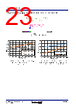
26 / 40 page  R34DS0017EU0104 Rev.1.04 Page 26 Jan 31, 2025 ISL73041SEH Datasheet 6.5 PVCC and BOOT Undervoltage Lockout (UVLO) The ISL73041SEH integrates a PVCC UVLO and a BOOT UVLO to prevent undervoltage gate drive to the half- bridge GaN FETs. The PVCC UVLO rising and falling thresholds are relative to the set voltage of PVCC, while the BOOT UVLO is at a fixed threshold. Under a PVCC UVLO condition, the high-side and low-side driver outputs do not respond to PWM input commands. Under a BOOT UVLO condition, only the high-side driver does not respond to PWM input commands. 6.6 Enable Control The EN pin controls the start-up of the driver. When EN = 0, the PVCC LDO is disabled. With no PVCC voltage, the FLT pin pulls low to indicate a driver's not-ready condition, and the driver outputs are in a high-impedance state. When EN = 1, the PVCC LDO is enabled, and if no other fault conditions exist, it releases the FLT pin and enables the driver outputs. The delay time between EN logic high and the PVCC LDO start-up is typically 115µs. The EN pin is VDD voltage compatible and can be tied to VDD for always-enabled applications. 6.7 PWM Operation Because of the tri-level input thresholds, the PWM pin is designed only for 0V to 5V logic level operation with a high-impedance float or external drive to establish the mid-level. In the high-impedance float state, internal pull-up and pull-down resistors bias the PWM pin at 2V. When PWM is logic high, the high-side driver is on, and the low-side driver is off. When PWM is logic low, the low-side driver is on, and the high-side driver is off. When PWM is at mid-level, both drivers are off. The PWM operating frequency range is limited on the low end by the boot capacitance on the BOOT to PHS pin to keep the boot circuit biased. As long as sufficient boot bias exists, there is no lower limit on the PWM frequency. The upper PWM frequency is limited by acceptable signal propagation and dead time delays. The typical minimum PWM pulse width for logic high and low to change the driver output state is 20ns. 6.8 Dead Time Control Resistor Setting The RDU and RDL pins set the rising edge dead time delay for the low-side and high-side drivers. The RDU pin controls UGH rising edge delay respective to the LGL falling edge. The RDL pin controls LGH rising edge delay respective to the UGL falling edge. A resistor to ground on RDU and RDL is required to set the dead time delay. A 1.2V reference voltage on RDU and RDL forces a current through the external resistors. This current is used to program the dead time delay. The dead time delay programmable range is from 6.5ns to 50ns using a 1.3kΩ to 10kΩ resistor. From the Typical Performance Curves Figure 14 and Figure 15, dead times beyond 50ns can be achieved, but the accuracy and dead-time matching performance is not guaranteed per the Electrical Specifications. Use Equation 2 to calculate the resistor value for a required dead time: Although not recommended due to no Electrical Performance testing with using resistance larger than 10kΩ, if using dead time larger than 50ns, use Equation 3 to determine resistor value. (EQ. 2) (EQ. 3) RDU or RDL k Dead Time ns 5.0 = RDU or RDL k Dead Time ns 6.5 + 5.4 = |
|
リンク URL |
| ALLDATASHEETはお客様のビジネスに役立ちますか? [ DONATE ] |
Alldatasheetは | 広告 | お問い合わせ | プライバシーポリシー | データシートへのリンク | リンク交換 | メーカーリスト All Rights Reserved©Alldatasheet.com |
| Russian : Alldatasheetru.com | Korean : Alldatasheet.co.kr | Spanish : Alldatasheet.es | French : Alldatasheet.fr | Italian : Alldatasheetit.com Portuguese : Alldatasheetpt.com | Polish : Alldatasheet.pl | Vietnamese : Alldatasheet.vn Indian : Alldatasheet.in | Mexican : Alldatasheet.com.mx | British : Alldatasheet.co.uk | New Zealand : Alldatasheet.co.nz |
|
Family Site : ic2ic.com |
icmetro.com |
 Japanese ▼
 English
 Chinese
 German
 Japanese
 Russian
 Korean
 Spanish
 French
 Italian
 Portuguese
 Polish
 Vietnamese
 Indian
 Mexican
 British
 New Zealand