|
データシートサーチシステム |
|
|
データシートサーチシステム |
|
ISL73847SEHDEMO2Z データシート(PDF) 33 Page - Renesas Technology Corp |
|
|
|||||||||||||||||||||||||||||
ISL73847SEHDEMO2Z データシート(HTML) 33 Page - Renesas Technology Corp |
|
|
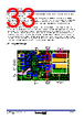
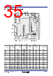
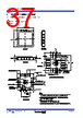
33 / 40 page  R34DS0017EU0104 Rev.1.04 Page 33 Jan 31, 2025 ISL73041SEH Datasheet ▪ Route the PHS pin to the switch node of the half-bridge power stage with a short and wide trace to minimize inductance and loop area. ▪ For the low-side drive, the PVCC capacitor, PVCC and PGND pins, low-side driver gate outputs, low-side FET gate, and GND plane form a current loop during FET turn on and turn off. For the high-side drive, the bootstrap capacitor, the BOOT and PHS pins, the high-side driver gate outputs, the high-side FET gate, and the switch node form a current loop during FET turn-on and turn-off. Keep these loops short and wide, and avoid overlapping with other sensitive signals. ▪ Size the phase node of the half-bridge (high-side FET source and low-side FET drain) area to handle the current and thermal dissipation from the FETs and switching load. The phase node copper area usually ends up being a significantly large shape. In addition, the phase node is where high voltage and high dv/dt switching occurs. In general, there are two layout practices for handling the phase node. One recommendation is to remove any conductors (including ground) that overlap the phase node on the adjacent layer of the PCB. The other recommendation is to repeat the phase node shape on every layer of the PCB. Both methods minimize the capacitive coupling of noise into the GND plane and prevent any sensitive analog signals from being routed underneath the phase node and causing unintentional common mode noise. 7.2 Layout Example RDU Resistor RDL Resistor AVCC Capacitor VDD Capacitor PVCC Capacitor BOOT Capacitor Upper Gate Resistors Lower Gate Resistors Upper GaN FET Lower GaN FET |
|
リンク URL |
| ALLDATASHEETはお客様のビジネスに役立ちますか? [ DONATE ] |
Alldatasheetは | 広告 | お問い合わせ | プライバシーポリシー | データシートへのリンク | リンク交換 | メーカーリスト All Rights Reserved©Alldatasheet.com |
| Russian : Alldatasheetru.com | Korean : Alldatasheet.co.kr | Spanish : Alldatasheet.es | French : Alldatasheet.fr | Italian : Alldatasheetit.com Portuguese : Alldatasheetpt.com | Polish : Alldatasheet.pl | Vietnamese : Alldatasheet.vn Indian : Alldatasheet.in | Mexican : Alldatasheet.com.mx | British : Alldatasheet.co.uk | New Zealand : Alldatasheet.co.nz |
|
Family Site : ic2ic.com |
icmetro.com |
 Japanese ▼
 English
 Chinese
 German
 Japanese
 Russian
 Korean
 Spanish
 French
 Italian
 Portuguese
 Polish
 Vietnamese
 Indian
 Mexican
 British
 New Zealand