データシートサーチシステム
  Japanese  ▼
ALLDATASHEET.JP

X  

33394 Datasheet with Chat AI
  • AIauthorized

    Hello, Please ask a question about 33394 Datasheet

  • # Example questions: ➢ What is the maximum allowable junction temperature for this device, and what are the thermal resistance values from junction to ambient (rθja) for the 44 hsop, 44 qfn, and 54 soicw-ep packages?
    ➢ What are the specified voltage limits for each of these standards?
    ➢ What is the acceptable range for the vbat supply voltage, and what is the maximum allowable output current for vddh?

  • Part No.33394
    ManufacturerFREESCALE
    Size639 Kbytes
    Pages44 pages
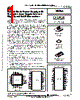
    DescriptionSwitch Mode Power Supply with Multiple Linear Regulators and High Speed CAN Transcelver
    Datasheet Summary with AI

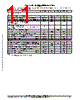
    1. Device Overview

    This appears to be a datasheet excerpt for a power management integrated circuit (PMIC), likely targeting automotive applications (given the emphasis on CAN bus robustness and load dump protection). It's a complex chip controlling multiple voltage rails and providing protection features.

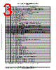
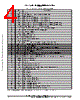
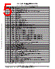
    2. Pin Descriptions (Based on information from the table)

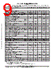
    ️· CANL/CANH: Communication pins, require robust ESD protection and transient voltage suppression.
    ️· /SLEEP: Likely an input to put the chip into a low-power mode.
    ️· REGON, VPP_EN, /HRESET, /PORESET, /PRERESET, HRT, DO, DI, CS, SCLK: Control and communication signals. Likely used to control the various regulators and communication protocols within the device. "/ " Prefix suggests active low signals.
    ️· CANTXD, CANRXD: Transmit/Receive pins for CAN communication.
    ️· VDDH, VDD3_3, VDDL, VKAM, VREF1, VREF2, VREF3, VSEN, VPRE: Voltage output rails with associated current ratings (see Recommended Operating Conditions).
    ️· DO, DI, CS, SCLK Digital I/O pins, probably related to SPI communication.

    3. Key Features (Inferred)

    ️· Multiple Voltage Regulation: Controls multiple voltage rails (VDDH, VDD3_3, VDDL, VKAM, etc.)
    ️· CAN Bus Protection: Built-in protection for CAN high and low lines, including ESD and transient voltage protection (load dump).
    ️· Protection Circuits: Includes protection against load dump, overvoltage, and other fault conditions.
    ️· Low Power Standby Mode: Implemented through the /SLEEP pin and VKAM output.
    ️· Communication Interfaces: Likely includes SPI (via DO, DI, CS, SCLK) and CAN interfaces.

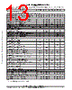
    4. Absolute Maximum Ratings

    These are *stress ratings* - exceeding them can cause permanent damage.

    Parameter Value (Typical Units)
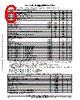
    VBAT/KA_VBAT/VIGN 4.0 - 26.5 V
    VDDH, VPP, VDD3_3, VDDL, VKAM -0.3 to +5.8 V
    VREF1, VREF2, VREF3, VSEN -2.0 to +18 V
    CAN Transient ± 200V
    Operating Temperature -40°C to +125°C
    Storage Temperature -65°C to +150°C
    Power Dissipation Up to 5W (depending on package)
    Lead Temperature (Soldering) 260°C (limited duration)

    5. Recommended Operating Conditions

    These define the intended operating ranges for reliable performance.

    Parameter Value Unit
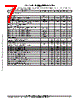
    VBAT/KA_VBAT 4.0 - 26.5 V
    VPRE (Switching Regulator Output Current) 0 - 1.2 A
    VDDH Output Current 0 - 400 mA
    VDD3_3 Output Current 0 - 120 mA
    VDDL Output Current 0 - 40 mA
    VKAM Output Current (Standby) 0-12 mA

    6. Important Notes and Cautions

    ️· ESD Sensitivity: The chip is sensitive to electrostatic discharge. Proper handling procedures are crucial.
    ️· Transient Protection: Special attention is required for the CAN bus, given the need for robust transient protection.
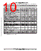
    ️· Thermal Management: Power dissipation and thermal resistance are critical considerations for reliable operation. Use appropriate heat sinks or thermal management techniques as needed. The provided Rθ values (thermal resistance) are essential for thermal design.
    ️· Voltage Limits: Exceeding the absolute maximum ratings can permanently damage the device.
    ️· Soldering: Lead soldering temperature is limited to 260°C for a short duration.


    Further Investigation Needed (based on the excerpt):

    ️· Complete Pinout and Functional Description: A full datasheet would provide a complete listing of all pins and their functions.
    ️· Detailed Circuit Diagrams: Understanding the internal architecture and regulation schemes requires circuit diagrams.
    ️· Application Examples: Example circuits and application notes would demonstrate how to use the device in typical automotive systems.
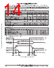
    ️· Timing Characteristics: Detailed timing information for communication interfaces (SPI, CAN) would be necessary for proper system integration.

    1. Device Overview

    This appears to be a datasheet excerpt for a power management integrated circuit (PMIC), likely targeting automotive applications (given the emphasis on CAN bus robustness and load dump protection). It's a complex chip controlling multiple voltage rails and providing protection features.

    2. Pin Descriptions (Based on information from the table)

    ️· CANL/CANH: Communication pins, require robust ESD protection and transient voltage suppression.
    ️· /SLEEP: Likely an input to put the chip into a low-power mode.
    ️· REGON, VPP_EN, /HRESET, /PORESET, /PRERESET, HRT, DO, DI, CS, SCLK: Control and communication signals. Likely used to control the various regulators and communication protocols within the device. "/ " Prefix suggests active low signals.
    ️· CANTXD, CANRXD: Transmit/Receive pins for CAN communication.
    ️· VDDH, VDD3_3, VDDL, VKAM, VREF1, VREF2, VREF3, VSEN, VPRE: Voltage output rails with associated current ratings (see Recommended Operating Conditions).
    ️· DO, DI, CS, SCLK Digital I/O pins, probably related to SPI communication.

    3. Key Features (Inferred)

    ️· Multiple Voltage Regulation: Controls multiple voltage rails (VDDH, VDD3_3, VDDL, VKAM, etc.)
    ️· CAN Bus Protection: Built-in protection for CAN high and low lines, including ESD and transient voltage protection (load dump).
    ️· Protection Circuits: Includes protection against load dump, overvoltage, and other fault conditions.
    ️· Low Power Standby Mode: Implemented through the /SLEEP pin and VKAM output.
    ️· Communication Interfaces: Likely includes SPI (via DO, DI, CS, SCLK) and CAN interfaces.

    4. Absolute Maximum Ratings

    These are *stress ratings* - exceeding them can cause permanent damage.

    Parameter Value (Typical Units)
    VBAT/KA_VBAT/VIGN 4.0 - 26.5 V
    VDDH, VPP, VDD3_3, VDDL, VKAM -0.3 to +5.8 V
    VREF1, VREF2, VREF3, VSEN -2.0 to +18 V
    CAN Transient ± 200V
    Operating Temperature -40°C to +125°C
    Storage Temperature -65°C to +150°C
    Power Dissipation Up to 5W (depending on package)
    Lead Temperature (Soldering) 260°C (limited duration)

    5. Recommended Operating Conditions

    These define the intended operating ranges for reliable performance.

    Parameter Value Unit
    VBAT/KA_VBAT 4.0 - 26.5 V
    VPRE (Switching Regulator Output Current) 0 - 1.2 A
    VDDH Output Current 0 - 400 mA
    VDD3_3 Output Current 0 - 120 mA
    VDDL Output Current 0 - 40 mA
    VKAM Output Current (Standby) 0-12 mA

    6. Important Notes and Cautions

    ️· ESD Sensitivity: The chip is sensitive to electrostatic discharge. Proper handling procedures are crucial.
    ️· Transient Protection: Special attention is required for the CAN bus, given the need for robust transient protection.
    ️· Thermal Management: Power dissipation and thermal resistance are critical considerations for reliable operation. Use appropriate heat sinks or thermal management techniques as needed. The provided Rθ values (thermal resistance) are essential for thermal design.
    ️· Voltage Limits: Exceeding the absolute maximum ratings can permanently damage the device.
    ️· Soldering: Lead soldering temperature is limited to 260°C for a short duration.


    Further Investigation Needed (based on the excerpt):

    ️· Complete Pinout and Functional Description: A full datasheet would provide a complete listing of all pins and their functions.
    ️· Detailed Circuit Diagrams: Understanding the internal architecture and regulation schemes requires circuit diagrams.
    ️· Application Examples: Example circuits and application notes would demonstrate how to use the device in typical automotive systems.
    ️· Timing Characteristics: Detailed timing information for communication interfaces (SPI, CAN) would be necessary for proper system integration.

    Part No.33394
    ManufacturerFREESCALE
    Size639 Kbytes
    Pages44 pages
    DescriptionSwitch Mode Power Supply with Multiple Linear Regulators and High Speed CAN Transcelver
    ALLDATASHEETはお客様のビジネスに役立ちますか?  [ DONATE ] 

    Alldatasheetは   |   広告   |   お問い合わせ   |   プライバシーポリシー   |   データシートへのリンク    |   リンク交換   |   メーカーリスト
    All Rights Reserved©Alldatasheet.com


    Mirror Sites
    English : Alldatasheet.com  |   English : Alldatasheet.net  |   Chinese : Alldatasheetcn.com  |   German : Alldatasheetde.com  |   Japanese : Alldatasheet.jp
    Russian : Alldatasheetru.com  |   Korean : Alldatasheet.co.kr  |   Spanish : Alldatasheet.es  |   French : Alldatasheet.fr  |   Italian : Alldatasheetit.com
    Portuguese : Alldatasheetpt.com  |   Polish : Alldatasheet.pl  |   Vietnamese : Alldatasheet.vn
    Indian : Alldatasheet.in  |   Mexican : Alldatasheet.com.mx  |   British : Alldatasheet.co.uk  |   New Zealand : Alldatasheet.co.nz
    Family Site : ic2ic.com  |   icmetro.com