|
データシートサーチシステム |
|
|
データシートサーチシステム |
|
33394 データシート(PDF) 29 Page - Freescale Semiconductor, Inc |
|
|
|||||||||||||||||||||||||||||
33394 データシート(HTML) 29 Page - Freescale Semiconductor, Inc |
|
|
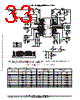
29 / 44 page  33394 29 MOTOROLA ANALOG INTEGRATED CIRCUIT DEVICE DATA After substitution, the calculated inductance value is L = 45 µH, which gives 47 µH standard component value. The peak–to peak ripple current value is: ∆IL = 0.345 A. The peak inductor current is given by: ILpk = 0.5∆IL + Io = 0.5x0.345 + 1.2 = 1.37[A] The inductor saturation current is given by the upper value of the 33394 internal switch current limit Ilim(max) = 3.0 A. Considering also the inductor serial resistance, these requirements are met, for example by the PO250.473T inductor from Pulse Engineering, Inc. 5.2.1.2. Selecting the Catch Diode D1 The rectifier D1 current capability has to be greater than calculated average current value. The maximum reverse voltage stress placed upon this rectifier D1 is given by maximum input voltage (maximum transient battery voltage). These requirements are met, for example by the HSM350 (3 A, 50 V) schottky diode from Microsemi, Inc. 5.2.1.3. Selecting the Output Capacitor The output capacitor Co should be a low ESR part, therefore the 100 µF tantalum capacitor with 80 mΩ ESR was chosen. From the formula for calculating the ripple voltage: VppESR = ∆IL x RESR = 0.345 x 0.08 = 28 [mV] One device that meets both, the low ESR, and the temperature stability requirements is, for example, the TPSV107K020R0085 tantalum capacitor from AVX Corp. Boost Converter Power Capability The boost converter with selected components has to be able to deliver the required power. Due to the nature of this non–compensated PFM control technique, the Boost converter output ripple voltage is higher than if it utilized a typical PWM control method. Therefore the switcher output voltage level is set higher than in the Buck mode (in the Boost mode VPRE = +6 V), in order to maintain a sufficient dropout voltage for the 5–volt linear regulators (VDDH, VREFs) and to avoid unwanted Resets to the microcontroller. The most stringent conditions for the 33394 boost converter occur with the lowest input voltage: Vin(min) = 3.5 V Io = 0.8 A Vpre = +6 V f = 200 kHz Vfwd1 = Vfwd2 = 0.5 V d = 0.75, duty cycle is fixed at 75% in boost mode Figure 16. 33394 Switcher Topology – Boost Mode IL VRES L Vin RLOAD VO + – + CO RD Q2 ESR D2 Vfwd2 IQ IL ILIM I01 I02 DIL1 < DIL2 Tt IL1 IL2 L1 > L2 IO1 > IO2 The input voltage drop associated with the resistance of the internal switch Q1 and inductor series resistance can be estimated as: VD [ Ipk(min) RD + 2.5 A 0.35 W + 0.875 V Where: VD is the voltage dissipated on the major parasitic resistances, RDSon of the internal power switch and inductor series resistance RL. For the worst case conditions: RD = RDSon(max) + RL = 0.25 + 0.1 = 0.35[Ω] Ipk(min) is the minimum internal power switch current limit value. Then the equation for calculating ∆IL can be modified as follows: DIL + Vin * VD L [(Vo ) Vfwd2) * (Vin * VD)] d (Vo ) Vfwd2) f + + 3.5 * 0.875 47 10*6 [(6 ) 0.5) * (3.5 * 0.875)] 0.75 (6 ) 0.5) 0.2 106 + 125[mA] Then the maximum average input current can be calculated as: IinAve + Ipk(min) * 1 2 DIL + 2.5 * 0.125 2 + 2.43[A] Finally, the boost converter power capability has to be higher than the required output power or: Pin(max) h u Pout Where Pin(max) is the boost converter maximum input power: h is the boost converter efficiency, in our case h is estimated to be h = 85%, and includes switching losses of the external power switch Q2 (MOSFET) inductor and capacitors AC losses, and output rectifier D2 (schottky) switching losses. Pout is the boost converter output power, which includes power loss of the output rectifier D2: Pout + (Vo ) Vfwd2) Io + (6 ) 0.5) 0.8 + 5.2[W] Pin + (Vin * VD) IinAve h + + (3.5 * 0.875) 2.43 0.85 + 5.42[W] As can be seen, the boost converter input power capability meets the required criteria. Freescale Semiconductor, Inc. For More Information On This Product, Go to: www.freescale.com |
|
リンク URL |
| ALLDATASHEETはお客様のビジネスに役立ちますか? [ DONATE ] |
Alldatasheetは | 広告 | お問い合わせ | プライバシーポリシー | データシートへのリンク | リンク交換 | メーカーリスト All Rights Reserved©Alldatasheet.com |
| Russian : Alldatasheetru.com | Korean : Alldatasheet.co.kr | Spanish : Alldatasheet.es | French : Alldatasheet.fr | Italian : Alldatasheetit.com Portuguese : Alldatasheetpt.com | Polish : Alldatasheet.pl | Vietnamese : Alldatasheet.vn Indian : Alldatasheet.in | Mexican : Alldatasheet.com.mx | British : Alldatasheet.co.uk | New Zealand : Alldatasheet.co.nz |
|
Family Site : ic2ic.com |
icmetro.com |
 Japanese ▼
 English
 Chinese
 German
 Japanese
 Russian
 Korean
 Spanish
 French
 Italian
 Portuguese
 Polish
 Vietnamese
 Indian
 Mexican
 British
 New Zealand