|
データシートサーチシステム |
|
|
データシートサーチシステム |
|
33394 データシート(PDF) 21 Page - Freescale Semiconductor, Inc |
|
|
|||||||||||||||||||||||||||||
33394 データシート(HTML) 21 Page - Freescale Semiconductor, Inc |
|
|
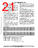
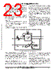
21 / 44 page  33394 21 MOTOROLA ANALOG INTEGRATED CIRCUIT DEVICE DATA 4.15. SPI Interface to Microcontroller (Serial Peripheral Interface) The pins specified for this function are: DI (Data Input), DO (Data Output), CS (Chip Select) and SCLK. Refer to Figure 3 for the 33394 SPI timing information. The delay, which is needed from CS leading edge active to the first SCLK leading edge transition (0 to 1) is approximately 125 ns. The SCLK rate is a maximum of 5.0 MHz. The SPI function will provide control of such 33394 features as VREFn regulator turn on/off, VREFn fault reporting and CAN wake up feature activation. Refer to Figure 7 & Figure 8 for the data and status bit assignments for the 16 bit SPI data word exchange. 4.15.1. CS (Chip Select) Pin The system MCU selects the 33394 to be communicated with through the use of the CS pin. Whenever the pin is in a logic high state, data can be transferred from the MCU to the 33394 and vice versa. Clocked—in data from the MCU is transferred to the 33394 shift register and latched in on the falling edge of the CS signal. On the rising edge of the CS signal, output status information is transferred from the output status register into the device’s shift register. Whenever the CS pin goes to a logic high state, the DO pin output is enabled allowing information to be transferred from the 33394 to the MCU. To avoid any spurious data, it is essential that the transition of the CS signal occur only when SCLK is in a logic low state. 4.15.2. SCLK (System Clock) Pin The shift clock pin (SCLK) clocks the internal shift registers of the 33394. The serial input (DI) data is latched into the input shift register on the rising edge of the SCLK. The serial output pin (DO) shifts data information out of the shift register also on the rising edge of the SCLK signal. It is essential that the SCLK pin be in a logic low state whenever the chip select pin (CS) makes any transition. For this reason, it is recommended though not necessary, that the SCLK pin is commanded to a low logic state as long as the device is not accessed (CS in logic low state). When CS is in a logic low state, any signal at the SCLK and DI pin is ignored and the DO is tri—stated (high impedance). 4.15.3. DI (Data Input) Pin The DI pin is used for serial data input. This information is latched into the input register on the rising edge of SCLK. A logic high state present on DI will program a specific function (see Figure 7 for the data bits assignments for the 16 bit SPI data word exchange.). The change will happen with the falling edge of the CS signal. To program the specific function of the 33394 a 16 bit serial stream of data is required to be entered into the DI pin starting with LSB. For each rising edge of the SCLK while CS is logic high, a data bit instruction is loaded into the shift register per the data bit DI state. The shift register is full after 16 bits of information have been entered. To preserve data integrity, care should be taken to not transition DI as SCLK transitions from a low to high logic state. 4.15.4. DO (Data Output) Pin The serial output (DO) pin is the output from the shift register. The DO pin remains tri—state until the CS pin goes to a logic high state. See Figure 8 for the status bits assignments for the 16–bit SPI data word exchange. The CS positive transition will make LSB status available on DO pin. Each successive positive SCLK will make the next bit status available. The DI/DO shifting of data follows a first—in—first—out protocol with both input and output words transferring the Least Significant Bit (LSB) first. 33394 SPI Registers: Serial Input Data/Control Default Value 0 0 0 0 0 0 0 0 Bit 15 14 13 12 11 10 9 8 Name Bit Definitions: Bit 15 to 8 = 0 Default Value 1 1 1 1 1 1 1 1 Bit 7 6 5 4 3 2 1 0 (LSB) Name WKUP CAN_EN VPP_V EN_VPP VSEN VREF3 VREF2 VREF1 Bit Definitions: Bit 7 — WKUP: WAKEUP activation. WKUP = 1: WAKEUP pin will signal CAN bus activity Bit 6 — CAN_EN: Enables CAN receiver, will draw small current during power off Bit 5 — VPP_V: Set VPP reference to 5V (1) or 3.3V (0), default is 5V Bit 4 — EN_VPP: – Used to turn the VPP regulator off and on from the MCU Bit 3 — VSEN: – Used to turn the VSEN regulator off and on from the MCU Bit 2 — VREF3: – Used to turn the VREF3 regulator off and on from the MCU Bit 1 — VREF2: – Used to turn the VREF2 regulator off and on from the MCU Bit 0 — VREF1: – Used to turn the VREF1 regulator off and on from the MCU Figure 7. SPI Input Data/ Control Register Freescale Semiconductor, Inc. For More Information On This Product, Go to: www.freescale.com |
|
リンク URL |
| ALLDATASHEETはお客様のビジネスに役立ちますか? [ DONATE ] |
Alldatasheetは | 広告 | お問い合わせ | プライバシーポリシー | データシートへのリンク | リンク交換 | メーカーリスト All Rights Reserved©Alldatasheet.com |
| Russian : Alldatasheetru.com | Korean : Alldatasheet.co.kr | Spanish : Alldatasheet.es | French : Alldatasheet.fr | Italian : Alldatasheetit.com Portuguese : Alldatasheetpt.com | Polish : Alldatasheet.pl | Vietnamese : Alldatasheet.vn Indian : Alldatasheet.in | Mexican : Alldatasheet.com.mx | British : Alldatasheet.co.uk | New Zealand : Alldatasheet.co.nz |
|
Family Site : ic2ic.com |
icmetro.com |
 Japanese ▼
 English
 Chinese
 German
 Japanese
 Russian
 Korean
 Spanish
 French
 Italian
 Portuguese
 Polish
 Vietnamese
 Indian
 Mexican
 British
 New Zealand