|
データシートサーチシステム |
|
|
データシートサーチシステム |
|
33394 データシート(PDF) 22 Page - Freescale Semiconductor, Inc |
|
|
|||||||||||||||||||||||||||||
33394 データシート(HTML) 22 Page - Freescale Semiconductor, Inc |
|
|
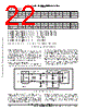
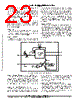
22 / 44 page  33394 22 MOTOROLA ANALOG INTEGRATED CIRCUIT DEVICE DATA 33394 SPI Registers: Serial Output Data/Status Default Value 0 0 0 0 0 0 0 0 Bit 15 14 13 12 11 10 9 8 Name Bit Definitions: Bit 15 to 8 = 0 Default Value 0 0 0 0 0 0 0 0 Bit 7 6 5 4 3 2 1 0 (LSB) Name VSEN–T VREF3–T VREF2–T VREF1–T VSEN–I VREF3–I VREF2–I VREF1–I Bit Definitions: Bit 7 — VSEN–T: – Will be set (1), if a thermal limit occurred since last SPI data transfer Bit 6 — VREF3–T: – Will be set (1), if a thermal limit occurred since last SPI data transfer Bit 5 — VREF2–T: – Will be set (1), if a thermal limit occurred since last SPI data transfer Bit 4 — VREF1–T: – Will be set (1), if a thermal limit occurred since last SPI data transfer Bit 3 — VSEN–I: – Will be set (1), if a current limit condition exists Bit 2 — VREF3–I: – Will be set (1), if a current limit condition exists Bit 1 — VREF2–I: – Will be set (1), if a current limit condition exists Bit 0 — VREF1–I: – Will be set (1), if a current limit condition exists NOTES: # individual thermal limit latch will clear on the trailing edge of the SPI CS signal Figure 8. SPI Output Data/ Status Register 4.16. CAN Transceiver The CAN protocol is defined in terms of ’dominant’ and ’recessive’ bits. When the digital input (CANTXD) is a logic ”0” (negated level, dominant bit), CANH goes to +3.5 V (nominal) and CANL goes to +1.5 V (nominal). The digital output will also be negated. When the digital input is logic ”1” (asserted level, recessive bit), CANH and CANL are set to +2.5 V (nominal). The corresponding digital output is also asserted. 4.16.1. CAN Network Topology There are two 120 Ω (only two), terminations between the CANH and CANL outputs. The majority of the time, the module controller will contain one of the terminations. The other termination should be as close to the other ”end” of the CAN Bus as possible. The termination provides a total of 60 Ω differential resistive impedance for generation of the voltage difference between CANH and CANL. Current flows out of CANH, through the termination, and then through CANL and back to ground. The CAN bus is not defined in terms of the bus capacitance. A filter capacitor of 220 pF to 470 pF may be required. The maximum capacitive load on the CAN bus is then 15 nF (not a lumped capacitance but distributed through the network cabling). Refer to Figure 9. Max : 31 Remotes CANH CANL PCM Vehicle Term. 120 W 120 W 470 pF* 470 pF* 470 pF* 470 pF* *Optional Common Mode Choke 2.2 mH Figure 9. CAN Load Characteristics 4.16.2. CAN Transceiver Functional Description A block diagram of the CAN transceiver is shown in Figure 10. A summary of the network topology is shown in Figure 9. The transceiver has wake up capability controlled by the state of the SPI bit WKUP. This allows 33394 to enter a low power mode and be awakened by CAN bus activity. When activity is sensed on the CAN bus pins, the 33394 will perform a power up sequence and will provide the microprocessor with indication (WAKEUP pin high) that wake up occurred from a CAN message. The 33394 may be placed back in low quiescent mode by pulling the /SLEEP pin from high to low. Freescale Semiconductor, Inc. For More Information On This Product, Go to: www.freescale.com |
|
リンク URL |
| ALLDATASHEETはお客様のビジネスに役立ちますか? [ DONATE ] |
Alldatasheetは | 広告 | お問い合わせ | プライバシーポリシー | データシートへのリンク | リンク交換 | メーカーリスト All Rights Reserved©Alldatasheet.com |
| Russian : Alldatasheetru.com | Korean : Alldatasheet.co.kr | Spanish : Alldatasheet.es | French : Alldatasheet.fr | Italian : Alldatasheetit.com Portuguese : Alldatasheetpt.com | Polish : Alldatasheet.pl | Vietnamese : Alldatasheet.vn Indian : Alldatasheet.in | Mexican : Alldatasheet.com.mx | British : Alldatasheet.co.uk | New Zealand : Alldatasheet.co.nz |
|
Family Site : ic2ic.com |
icmetro.com |
 Japanese ▼
 English
 Chinese
 German
 Japanese
 Russian
 Korean
 Spanish
 French
 Italian
 Portuguese
 Polish
 Vietnamese
 Indian
 Mexican
 British
 New Zealand