|
データシートサーチシステム |
|
|
データシートサーチシステム |
|
33394 データシート(PDF) 17 Page - Freescale Semiconductor, Inc |
|
|
|||||||||||||||||||||||||||||
33394 データシート(HTML) 17 Page - Freescale Semiconductor, Inc |
|
|
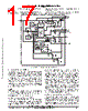
17 / 44 page  33394 17 MOTOROLA ANALOG INTEGRATED CIRCUIT DEVICE DATA 4.2.6. Switching Regulator Output Voltage Sense (VPRE_S) This is the switching regulator output voltage sense input. The switcher output voltage VPRE is divided by an internal resistor divider and compared with the bandgap reference voltage (see Figure 4). Refer to Section 5 Application Information for detailed description of the switching regulator operation. Figure 4. Switching Regulator Block Diagram BUCK & BOOST CONTROL LOGIC CURRENT LIMIT SOFT START + – – + FEED FORWARD RAMP GENERATOR THERMAL LIMIT SWITCHER OSCILLATOR 200 kHz SWITCHER MODE ENABLE Vbg + – PWM COMP Vbg Vbg VPRE COMP BOOTSTRAP VBAT + – BOOST COMP Vbg 1.25 V Vbg 1.25 V Vbg 1.25 V E/A LS DRIVER HS DRIVER VPRE VPRE BOOT SW1 VPRE SW2G VPRE_S INV VCOMP 40 k 11.7 k 4.3. Voltage Regulator (VDDH) The VDDH output is a linearly regulated +5.0 +/– 0.10V voltage supply capable of sourcing a maximum of 400 mA steady state current from VPRE (+5.6 V) for VBAT voltages from +4.0 V to +26.5 V (+45V transient). This regulator incorporates current limit short circuit protection and thermal shut down protection. The voltage output is stable under all load/line conditions. However, the designer must consider ripple and high frequency filtering as well as regulator response, when choosing external components. See Table 1 in the Applications Information section for recommended output capacitor parameters. NOTE : Backfeeding into the VDDH output can cause problems during the power up sequence. Refer to the Electrical Characteristics VDDH Regulator Section for the maximum allowed backfed current into the VDDH output. 4.4. Tracking Voltage Regulator (VPP) This linearly regulated +5.0 V/+3.3 V (SPI selectable) voltage supply is capable of sourcing 150 mA of steady state current from VPRE (+5.6 V) for VBAT voltage from +4.0 V to +26.5 V (up to +45V transient). It tracks the VDDH or VDD3_3 output, and incorporates current limit short circuit protection and over temperature shut down protection. This output is intended for FLASH memory programming and includes a dedicated enable pin (VPP_EN). The regulator enable can also be controlled through the SPI interface but requires both the VPP_EN pin and the SPI bit (EN_VPP bit) to be high to enable. The selection of tracking VDDH or VDD3_3 is controlled by the VPP_V bit in the SPI. Logic “1” selects VDDH (default), logic “0” selects VDD3_3. The voltage output is stable under all load/line conditions. However, the designer must consider ripple and high frequency filtering as well as regulator response when choosing external components. See Table 1 for recommended output capacitor parameters. The VPP tracking regulator should not be used in parallel with the VDDH regulator, because this arrangement can corrupt the proper power sequencing of the IC. 4.5. Tracking Voltage Regulator (VREFn) The outputs of the VREF1, VREF2, VREF3 linear regulators are 100 mA at +5.0 V. They track the VDDH output. The power supplies are designed to supply power to sensors that are located external to the module. These regulators may be enabled or disabled via the SPI, which also provides fault reporting for these regulators. They are protected for short to Freescale Semiconductor, Inc. For More Information On This Product, Go to: www.freescale.com |
|
リンク URL |
| ALLDATASHEETはお客様のビジネスに役立ちますか? [ DONATE ] |
Alldatasheetは | 広告 | お問い合わせ | プライバシーポリシー | データシートへのリンク | リンク交換 | メーカーリスト All Rights Reserved©Alldatasheet.com |
| Russian : Alldatasheetru.com | Korean : Alldatasheet.co.kr | Spanish : Alldatasheet.es | French : Alldatasheet.fr | Italian : Alldatasheetit.com Portuguese : Alldatasheetpt.com | Polish : Alldatasheet.pl | Vietnamese : Alldatasheet.vn Indian : Alldatasheet.in | Mexican : Alldatasheet.com.mx | British : Alldatasheet.co.uk | New Zealand : Alldatasheet.co.nz |
|
Family Site : ic2ic.com |
icmetro.com |
 Japanese ▼
 English
 Chinese
 German
 Japanese
 Russian
 Korean
 Spanish
 French
 Italian
 Portuguese
 Polish
 Vietnamese
 Indian
 Mexican
 British
 New Zealand