|
データシートサーチシステム |
|
|
データシートサーチシステム |
|
33394 データシート(PDF) 16 Page - Freescale Semiconductor, Inc |
|
|
|||||||||||||||||||||||||||||
33394 データシート(HTML) 16 Page - Freescale Semiconductor, Inc |
|
|
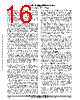
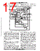
16 / 44 page  33394 16 MOTOROLA ANALOG INTEGRATED CIRCUIT DEVICE DATA 4. FUNCTIONAL DESCRIPTION The 33394 is an integrated buck regulator/linear supply specifically designed to supply power to the Motorola MPC55x/MPC56x microprocessors. A detailed functional description of the Buck Regulator, Linear Regulators, Power Up/Down Sequences, Thermal Shutdown Protection, Can Transceiver Reset Functions and Reverse Battery Function are given below. Block diagram of the 33394 is given in Figure 1. The 33394 is packaged in a 44 pin HSOP, 54 pin SOICW and the 44 pin QFN. 4.1. Input Power Source (VBAT, KA_VBAT & VIGN) The VBAT and KA_VBAT pins are the input power source for the 33394. The VBAT pins must be externally protected from vehicle level transients greater than +45 V and reverse battery. See typical application diagram in Figure 1. The VBAT pins directly supply the pre–regulator switching power supply. All power to the linear regulators (except VKAM in the power down mode) is supplied from VBAT through the switching regulator. VKAM power is supplied through VBAT input pins and switching regulator when the 33394 is awake. When the microprocessor is in a power down mode (no VDDH or VDDL supply), the current requirement on VKAM falls to less than 12 mA. During this period the VKAM current is supplied from the reverse battery protected KA_VBAT input. The KA_VBAT supply pin is the power source to the Keep Alive Memory regulator (VKAM) in power down mode. Power is continuously supplied regardless of the state of the ignition switch (VIGN input). The KA_VBAT input is reverse battery protected but requires external load dump protection (refer to Figure 1). The VIGN pin is used as a control input to the 33394. The regulation circuits will function and draw current from VBAT when VIGN is high (active) or REGON is high (active) or on CAN bus activity (WAKEUP active). To keep the VIGN input from floating, a 10k W pull–down resistor to GND should be used. The VIGN pin has a 3.0 V threshold and 1.0 volt of hysteresis. VIGN is designed to operate up to +26.5 volt battery while providing reverse battery and +45 volt load dump protection. The input requires ESD, and transient protection. See Figure 1 for external component required. 4.2. Switching Regulator Functional Description A block diagram of the internal switching regulator is shown in Figure 4. The switching regulator incorporates circuitry to implement a Buck or a Buck/Boost regulator with additional external components. A high voltage, low RDS(on) power MOSFET is included on chip to minimize the external components required to implement a Buck regulator. The power MOSFET is a sense FET to implement current limit. For low voltage operation, a low side driver is provided that is capable of driving external logic level MOSFETs. This allows a switching regulator utilizing Buck/Boost topology to be implemented. Two independent control schemes are utilized in the switching regulator. In Buck mode, voltage mode pulse–width modulation (PWM) control is used. The switcher output voltage divided by an internal resistor divider is sensed by an Error Amplifier and compared with the bandgap reference voltage. The PWM Comparator uses the output signal from the Error Amplifier as the threshold level. The PWM Comparator compares the sawtooth voltage from the Ramp Generator with the output signal from the Error Amplifier thus creating a PWM signal to the control logic block. The Error Amplifier inverting input and output are brought out to enable the control loop to be externally compensated. The compensation technique is described in paragraph 5.2.3. Buck Converter Feedback Compensation in the Application Information section. In order to improve line rejection, feed forward is implemented in the ramp generator. The feed forward modifies the ramp slope in proportion to the VBAT voltage in a manner to keep the loop gain constant, thus simplifying loop compensation. At startup, a soft start circuit lowers the current limit value to prevent potentially destructive in–rush current. In Boost mode, pulse–frequency modulation (PFM) control is utilized. The duty cycle is set to 75% and the switching action is stopped either by the Boost Comparator, sensing the switcher output voltage VPRE, or by the Current Limit circuit when the switching current reaches its predetermined limit value. This control method requires no external components. The selection of the control method is determined by the control logic based on the VBAT input voltage. 4.2.1. Switching Transistor (SW1) The internal switching transistor is an n–channel power MOSFET. The RDS(on) of this internal power FET is approximately 0.25 ohm at +125 _C. The 33394 has a nominal instantaneous current limit of 3.0 A (well below the saturation current of the MOSFET and external surface mounted inductor) in order to supply 1.2 A of current for the linear regulators that are connected to the VPRE pin (see Figure 1). The input to the drain of the internal N—channel MOSFET must be protected by an external series blocking diode, for reverse battery protection (see Figure 1). 4.2.2. Bootstrap Pin (BOOT) An external bootstrap 0.1 µF capacitor connected between SW1 and the BOOT pin is used to generate a high voltage supply for the high side driver circuit of the buck controller. The capacitor is pre charged to approximately 10V while the internal FET is off. On switching, the SW1 pin is pulled up to VBAT, causing the BOOT pin to rise to approximately VBAT+10V — the highest voltage stress on the 33394. 4.2.3. External MOSFET Gate Drive (SW2G) This is an output for driving an external FET for boost mode operation. Due to the fact that the gate drive supply voltage is VPRE the external power MOSFET should be a logic level device. It also has to have a low RDS(on) for acceptable efficiency. During buck mode, this gate output is held low. 4.2.4. Compensation (INV, VCOMP) The PWM error amplifier inverting input and output are brought out to allow the loop to be compensated. The recommended compensation network is shown in Figure 18 and its Bode plot is in Figure 19. The use of external compensation components allows optimization of the buck converter control loop for the maximum bandwidth. Refer to the paragraph 5.2.3. Buck Converter Feedback Compensation in the Application Information section for further details of the buck controller compensation. 4.2.5. Switching Regulator Output Voltage (VPRE) The output of the switching regulator is brought into the chip at the VPRE pin. This voltage is required for both the switching regulator control and as the supply voltage for all the linear regulators. Freescale Semiconductor, Inc. For More Information On This Product, Go to: www.freescale.com |
|
リンク URL |
| ALLDATASHEETはお客様のビジネスに役立ちますか? [ DONATE ] |
Alldatasheetは | 広告 | お問い合わせ | プライバシーポリシー | データシートへのリンク | リンク交換 | メーカーリスト All Rights Reserved©Alldatasheet.com |
| Russian : Alldatasheetru.com | Korean : Alldatasheet.co.kr | Spanish : Alldatasheet.es | French : Alldatasheet.fr | Italian : Alldatasheetit.com Portuguese : Alldatasheetpt.com | Polish : Alldatasheet.pl | Vietnamese : Alldatasheet.vn Indian : Alldatasheet.in | Mexican : Alldatasheet.com.mx | British : Alldatasheet.co.uk | New Zealand : Alldatasheet.co.nz |
|
Family Site : ic2ic.com |
icmetro.com |
 Japanese ▼
 English
 Chinese
 German
 Japanese
 Russian
 Korean
 Spanish
 French
 Italian
 Portuguese
 Polish
 Vietnamese
 Indian
 Mexican
 British
 New Zealand