|
データシートサーチシステム |
|
|
データシートサーチシステム |
|
33394 データシート(PDF) 26 Page - Freescale Semiconductor, Inc |
|
|
|||||||||||||||||||||||||||||
33394 データシート(HTML) 26 Page - Freescale Semiconductor, Inc |
|
|
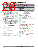
26 / 44 page  33394 26 MOTOROLA ANALOG INTEGRATED CIRCUIT DEVICE DATA Table 1. Linear Regulator Output Capacitor Examples Output SMD tantalum Value/Rating Part n. (AVX Corp.) VDDH 100uF/10V TPSC107K010S0200 VPP 33uF/10V TPSB336K010S0650 VDD3_3 68uF/6.3V TPSC686K006S0200 VDDL 100uF/6.3V TPSC107K006S0150 VREFx 10uF/16V THJB106K016S VKAM* 100uF/6.3V TPSC107K006S0150 5.2. Switching Regulator Operation The 33394 switching regulator circuit consists of two basic switching converter topologies. One is the typical voltage mode PWM step–down or buck regulator, which provides pre–regulated VPRE voltage (+5.6 V) during normal operating conditions. During cold start–up, when the car battery is weak, the input voltage for the 33394 can fall below the lower operating limit of the step–down converter. Under such conditions, the step–up or boost converter provides the required value of the VPRE voltage. The following paragraphs describe the basic principles of the two converters operation. Buck Mode One switching cycle of the step–down converter operation has two distinct parts: the power switch on state and the off state. When the power switch is on, one inductor terminal is connected to the input voltage Vin, and the other inductor terminal is the output voltage Vo. During this part of the switching period the rectifier (catch diode) is back biased, and the current ramps up through the inductor to the output: iL(on) + (Vin * Vo) ton L Where: ton is the on–time of the power switch. Vin is the input voltage. Vo is the output voltage. iL(on) is the inductor current during the on–time. L is the inductance of the inductor L. During the on time, current ramping through the inductor stores energy in the inductor core. During the off time of the power switch, the input voltage source Vin is disconnected from the circuit. The energy stored in the core forces current to continue to flow in the same direction, the rectifier is forward biased and the inductor input voltage is clamped one forward diode drop below ground. The inductor current during the off time is: iL(off) + (Vo * Vfwd) toff L Where: toff is the off–time of the power switch. iL(off) is the inductor current during the off time. Vfwrd is forward voltage drop across the rectifier. During the steady state operation iL(on) = iL(off) = ∆IL, and Vin/Vo = d Where: d is the duty cycle, and d = ton/T. T is switching period, T = 1/f. f is the frequency of operation. Two relations give the ripple voltage in the output capacitor Co. The first describes ripple voltage caused by current variation upon the output capacitance Co: VppCo + DIL 8Co f The other is caused by current variations over the output capacitor equivalent series resistance ESR: VppESR + DIL RESR Practically, the ESR contributes predominantly to the buck converter ripple voltage: VppESR >>VppCo The inductor peak current can be calculated as follows: IpkL + Io ) 1 2 DIL Where: Io is the average output current. Freescale Semiconductor, Inc. For More Information On This Product, Go to: www.freescale.com |
|
リンク URL |
| ALLDATASHEETはお客様のビジネスに役立ちますか? [ DONATE ] |
Alldatasheetは | 広告 | お問い合わせ | プライバシーポリシー | データシートへのリンク | リンク交換 | メーカーリスト All Rights Reserved©Alldatasheet.com |
| Russian : Alldatasheetru.com | Korean : Alldatasheet.co.kr | Spanish : Alldatasheet.es | French : Alldatasheet.fr | Italian : Alldatasheetit.com Portuguese : Alldatasheetpt.com | Polish : Alldatasheet.pl | Vietnamese : Alldatasheet.vn Indian : Alldatasheet.in | Mexican : Alldatasheet.com.mx | British : Alldatasheet.co.uk | New Zealand : Alldatasheet.co.nz |
|
Family Site : ic2ic.com |
icmetro.com |
 Japanese ▼
 English
 Chinese
 German
 Japanese
 Russian
 Korean
 Spanish
 French
 Italian
 Portuguese
 Polish
 Vietnamese
 Indian
 Mexican
 British
 New Zealand