|
データシートサーチシステム |
|
|
データシートサーチシステム |
|
33394 データシート(PDF) 30 Page - Freescale Semiconductor, Inc |
|
|
|||||||||||||||||||||||||||||
33394 データシート(HTML) 30 Page - Freescale Semiconductor, Inc |
|
|
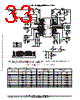
30 / 44 page  33394 30 MOTOROLA ANALOG INTEGRATED CIRCUIT DEVICE DATA 5.2.1.4. Selecting the Power MOSFET Q2 The boost converter maximum output voltage plus the voltage drop across the output schottky rectifier D2 gives the MOSFET’s maximum drain–source voltage stress: BVdsQ2>Vo+Vfwd2 = 6 V+0.5 V, as can be seen, the breakdown voltage parameter is not critical. The more important in our case is the Q2 current handling capability. The external power MOSFET has to withstand higher currents than the upper current limit of the 33394: IDQ2>3A In order to keep the power dissipation of the 33394 boost converter to its minimum, a very low RDSon power MOSFET has to be selected. Moreover, due to the fact that the 33394 external MOSFET gate driver is supplied from VPRE, in order to assure proper switching of Q2 a logic level device has to be selected. Last but not least, the Q2 package has to suitable for the harsh automotive environment with low thermal resistance. These requirements are met, for example by the MTD20N03HDL power MOSFET from ON Semiconductor. 5.2.1.5. Selecting the Boost Converter Output Rectifier D2 Criteria similar to that of selecting the power MOSFET was used to select the boost converter output rectifier. Its reverse breakdown voltage is not a critical parameter: VrD2>Vo=6 V The D2 rectifier has to withstand higher peak current than is the 33394 internal switch upper current limit Ilim(max). The most important parameter is its forward voltage drop, which has to be minimal. This parameter is also crucial for the proper 33394 switcher functionality, and especially for proper transition between the buck and boost modes. Finally, its switching speed, forward and reverse recovery parameters play a significant role when selecting the output rectifier D2. These requirements are met, for example by the HSM350 schottky rectifier from Microsemi, Inc. 5.2.2. Input Filter Selection Since the switcher will work in the Boost mode only during cold crank condition, the 33394 EMC (electromagnetic compatibility) performance is not of concern during this mode of operation. Therefore, only the Buck mode of operation is important for selecting the appropriate input filter. For the Buck converter topology (see Figure 13) the low impedance 3rd order filter (C3, L2, C4 and C26 in the Application Schematic Diagram Figure 20) offers a good solution. It can be seen from the Buck converter current waveforms that comparatively high current pulses are drawn from the converter’s input source. The filter inductance must be kept minimal and the capacitor, which is placed right next to the power switch, must be sized large enough to provide sufficient energy reservoir for proper switcher operation. The ESR of this input capacitor combination C4, C26 has to be sufficiently low to reduce the switching ripple of the switcher input node VBAT. There are three main reasons to keep the voltage ripple of the VBAT pin at its minimum. First, it is the EMC (electromagnetic compatibility) performance of the switcher in the normal operating mode (buck mode). Second, it allows a smooth transition between the boost and buck mode of operation. Third, it helps to avoid entering an undervoltage condition too early. A practical way to achieve sufficiently low ESR of the switcher input capacitor, even at low temperature extremes, is to use several high value ceramic capacitors in parallel with a large electrolytic capacitor. These capacitors should be physically placed as close to the VBAT pins as possible. 5.2.3. Buck Converter Feedback Compensation A typical control loop of the buck regulator is shown in Figure 17. The loop consists of a power processing block — the modulator in series with an error–detecting block — the Error (Feedback) Amplifier. In principle, a portion of the output voltage (VPRE of the 33394 switcher) is compared to a reference voltage (Vbg) in the Error Amplifier and the difference is amplified and inverted and used as a control input for the modulator to keep the controlled variable (output voltage VPRE) constant. Figure 17. The Buck Converter Control Loop – + + – + Zin Zf Reference Voltage ERROR FEEDBACK AMPLIFIER MODULATOR Vout To Load Ramp PWM Signal Vin Gain Block (Modulator) Feedback Block G H S Vout Vin + – Vout/Vin = G/(1 + GH) Freescale Semiconductor, Inc. For More Information On This Product, Go to: www.freescale.com |
|
リンク URL |
| ALLDATASHEETはお客様のビジネスに役立ちますか? [ DONATE ] |
Alldatasheetは | 広告 | お問い合わせ | プライバシーポリシー | データシートへのリンク | リンク交換 | メーカーリスト All Rights Reserved©Alldatasheet.com |
| Russian : Alldatasheetru.com | Korean : Alldatasheet.co.kr | Spanish : Alldatasheet.es | French : Alldatasheet.fr | Italian : Alldatasheetit.com Portuguese : Alldatasheetpt.com | Polish : Alldatasheet.pl | Vietnamese : Alldatasheet.vn Indian : Alldatasheet.in | Mexican : Alldatasheet.com.mx | British : Alldatasheet.co.uk | New Zealand : Alldatasheet.co.nz |
|
Family Site : ic2ic.com |
icmetro.com |
 Japanese ▼
 English
 Chinese
 German
 Japanese
 Russian
 Korean
 Spanish
 French
 Italian
 Portuguese
 Polish
 Vietnamese
 Indian
 Mexican
 British
 New Zealand