|
データシートサーチシステム |
|
|
データシートサーチシステム |
|
33394 データシート(PDF) 27 Page - Freescale Semiconductor, Inc |
|
|
|||||||||||||||||||||||||||||
33394 データシート(HTML) 27 Page - Freescale Semiconductor, Inc |
|
|
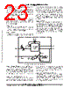
27 / 44 page  33394 27 MOTOROLA ANALOG INTEGRATED CIRCUIT DEVICE DATA Figure 13. Basic Buck Converter Operation and its Waveforms IQ IL ID D Q Vin RLOAD VO + – + CO L Vin RLOAD + – + CO L POWER SWITCH ON ILOAD Vout ILO VD(fwd) RLOAD + – + CO POWER SWITCH OFF ILOAD Vout ILO IO IL IQ –ID VD VCo DIL ton toff T Vfwd t Boost Mode The operation of the boost converter also consists of two parts, when the power switch is on and off. When the power switch turns on, the input voltage source is placed directly across the inductor, and the current ramps up linearly through the inductor as described by: iL(on) + Vin ton L Where: ton is the on–time of the power switch. Vin is the input voltage. iL(on) is the inductor current during the on–time. L is the inductance of the inductor L. The current ramping across the inductor stores energy within the core material. In order to maintain steady–state operation, the amount of energy stored during each switching cycle, times the frequency of operation must be higher (to cover the losses) than the power demands of the load: Psto + 1 2 LI2pk f u Pout When the power switch turns off again, the inductor voltage flies back above the input voltage and is clamped by the forward biased rectifier at the output voltage. The current ramps down through the inductor to the output until the new on time begins or, in case of discontinuous mode of operation, until the energy stored in the inductor core drops to zero. iL(off) + (Vo * Vin) toff L Where: toff is the off–time of the power switch. Vo is the output voltage. During the steady state operation iL(on) = iL(off) = ∆IL, and d + Vo * Vin Vo Where: d is the duty cycle, and d = ton/T. T is switching period, T = 1/f. f is the frequency of operation. The ripple voltage of the boost converter can be described as: VppCo + Io Co (Vo * Vin) Vo f Where: VppCo is the ripple caused by output current. The portion of the output ripple voltage caused by the ESR of the output capacitor is: VppESR + (Io Vo Vin ) 1 2 DIL) RESR Freescale Semiconductor, Inc. For More Information On This Product, Go to: www.freescale.com |
|
リンク URL |
| ALLDATASHEETはお客様のビジネスに役立ちますか? [ DONATE ] |
Alldatasheetは | 広告 | お問い合わせ | プライバシーポリシー | データシートへのリンク | リンク交換 | メーカーリスト All Rights Reserved©Alldatasheet.com |
| Russian : Alldatasheetru.com | Korean : Alldatasheet.co.kr | Spanish : Alldatasheet.es | French : Alldatasheet.fr | Italian : Alldatasheetit.com Portuguese : Alldatasheetpt.com | Polish : Alldatasheet.pl | Vietnamese : Alldatasheet.vn Indian : Alldatasheet.in | Mexican : Alldatasheet.com.mx | British : Alldatasheet.co.uk | New Zealand : Alldatasheet.co.nz |
|
Family Site : ic2ic.com |
icmetro.com |
 Japanese ▼
 English
 Chinese
 German
 Japanese
 Russian
 Korean
 Spanish
 French
 Italian
 Portuguese
 Polish
 Vietnamese
 Indian
 Mexican
 British
 New Zealand