|
データシートサーチシステム |
|
|
データシートサーチシステム |
|
33394 データシート(PDF) 18 Page - Freescale Semiconductor, Inc |
|
|
|||||||||||||||||||||||||||||
33394 データシート(HTML) 18 Page - Freescale Semiconductor, Inc |
|
|
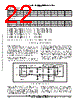
18 / 44 page  33394 18 MOTOROLA ANALOG INTEGRATED CIRCUIT DEVICE DATA battery (+18 V) and short to –2.0 V. Precautions must be taken to protect the VREF pins from exposure to transients. See Table 1 for recommended output capacitor parameters. 4.5.1. VREF Over Temperature Latch Off Feature If either the VREF1, VREF2 or VREF3 outputs is shorted to ground for any duration of time, an over temperature shut down circuit disables the output source transistor once the local die temperature exceeds +150 °C to +190°C. The output transistor remains off until the locally sensed temperature is 5 °C to 20°C. below the trip off temperature. The output(s) will periodically turn on and off until either the die temperature decreases or until the fault condition is removed. If one of these outputs goes into over—temperature shutdown, it will not impact the operation of any of the other outputs (assuming that no other package thermal or VPRE current limit specifications are violated). Fault information is reported through the SPI communication interface (see Figure 8). 4.6. Voltage Regulator (VDD3_3) This linearly regulated +3.3 V +/–0.06 V voltage supply is capable of sourcing 120 mA of steady state current from VPRE (+5.6 V) for VBAT voltage from +4.0 V to +26.5 V (+45V transient). This regulator incorporates current limit short circuit protection and thermal protection. When no external pass transistor is used the VDD3_3 and the VDD3_3FB pins must be shorted together — see Figure 22. The current capability of the VDD3_3 output can be increased by means of an external pass transistor — see Figure 1. When the external pass transistor is used the VDD3_3 internal short circuit current limit does not provide the short circuit protection. The voltage output is stable under all load/line conditions. However, the designer must consider ripple and high frequency filtering as well as regulator response when choosing external components. See Table 1 in the Applications Information section for recommended output capacitor parameters. NOTE : Backfeeding into the VDD3_3 output can cause problems during the power up sequence. Refer to the Electrical Characteristics VDD3_3 Regulator Section for the maximum allowed backfed current into the VDD3_3 output. 4.7. Voltage Regulator (VDDL) The output voltage of the VDDL linear regulator is adjustable by means of an external resistor divider. This linearly regulated +/–2% core voltage supply uses an external pass transistor and is capable of sourcing 40 mA base drive current typically (see application circuit, Figure 1) of steady state current. The collector of the external NPN pass transistor is connected to VPRE (+5.6 V) for a VBAT voltage from +7.5 V to +26.5 V (+45V transient). The voltage output is stable under all load/line conditions. However, the designer must consider ripple and high frequency filtering as well as regulator response when choosing external components. Also, the dynamic load characteristics of the microprocessor, relative to CPU clock frequency changes must be considered. An additional external pass transistor, for VDDL regulation in the Boost mode, can be added between protected battery voltage (see Figure 1) and VDDL, with its base driven by VDDL_X. In that arrangement the 33394’s core voltage supply operates over the whole input voltage range VBAT = +4.0 V to +26.5 V (up to +45V transient). See Table 1 in the Applications Information section for recommended output capacitor parameters. NOTES: 1. The use of an EXTERNAL pass device allows the power dissipation of the 33394 to be reduced by approximately 50% and thereby allows the use of a thermally efficient package such as an HSOP 44 or QFN 44. The base drive control signal (VDDL_B) is provided by on chip circuitry. The regulated output voltage sense signal is fed back into the on chip differential amplifier through pin VDDL_FB. The collector of this external pass device should be connected to VPRE to minimize power dissipation and adequately supply 400 mA. Proper thermal mounting considerations must be accounted for in the PCB design. 2. Backfeeding into the VDDL output can cause problems during the power up sequence. Refer to the Electrical Characteristics VDDL Regulator Section for the maximum allowed backfed current into the VDDL output. 4.8. Keep–Alive/Standby Supply (VKAM) This linearly regulated Keep Alive Memory voltage supply tracks the VDDL (+1.25 V to +3.3 V) core voltage, and is capable of sourcing 50 mA of steady state current from VPRE during normal microprocessor operation and 12 mA through KA_VBAT pin during stand–by/sleep mode. The VKAM regulator output incorporates a current limit short circuit protection. The output requires a specific range of capacitor values to be stable under all load/line conditions. See Table 1 in the Applications Information section for recommended output capacitor parameters. NOTE : The source current for the VKAM supply output depends on the sleep/wake state of the 33394. 4.9. Switched Battery Output (VSEN) This is a saturated switch output, which tracks the VBAT and is capable of sourcing 125 mA of steady state current from VBAT. This regulator will track the voltage VBAT to less than 200 mV, and its output voltage is clamped at +17 V. The gate voltage of the internal N—channel MOSFET is provided by a charge pump from VBAT. There is an internal gate–to–source voltage clamp. This regulator is short circuit protected and has independent over—temperature protection. If this output is shorted and goes into thermal shutdown, the normal operation of all other voltage outputs is not impacted. This output is controlled by the SPI VSEN bit. NOTE: A short to VBAT on VREF1, VREF2, VREF3 or VSEN will not result in additional current being drawn from the battery under normal (+8 V to +18 V) voltage levels. Under jumpstart condition (VBAT = +26.5 V) and during load dump condition, the device will survive this condition, but additional current may be drawn from the battery. 4.9.1. VSEN Over Temperature Latch Off Feature If the VSEN output is shorted to ground for any duration of time, an over temperature shut down circuit disables the output source transistor once the local die temperature exceeds +150 °C to +190°C. The output transistor remains off until the locally sensed temperature drops 5 °C to 20°C below Freescale Semiconductor, Inc. For More Information On This Product, Go to: www.freescale.com |
|
リンク URL |
| ALLDATASHEETはお客様のビジネスに役立ちますか? [ DONATE ] |
Alldatasheetは | 広告 | お問い合わせ | プライバシーポリシー | データシートへのリンク | リンク交換 | メーカーリスト All Rights Reserved©Alldatasheet.com |
| Russian : Alldatasheetru.com | Korean : Alldatasheet.co.kr | Spanish : Alldatasheet.es | French : Alldatasheet.fr | Italian : Alldatasheetit.com Portuguese : Alldatasheetpt.com | Polish : Alldatasheet.pl | Vietnamese : Alldatasheet.vn Indian : Alldatasheet.in | Mexican : Alldatasheet.com.mx | British : Alldatasheet.co.uk | New Zealand : Alldatasheet.co.nz |
|
Family Site : ic2ic.com |
icmetro.com |
 Japanese ▼
 English
 Chinese
 German
 Japanese
 Russian
 Korean
 Spanish
 French
 Italian
 Portuguese
 Polish
 Vietnamese
 Indian
 Mexican
 British
 New Zealand