|
データシートサーチシステム |
|
|
データシートサーチシステム |
|
H8SX/1663R データシート(PDF) 290 Page - Renesas Technology Corp |
|
|
|||||||||||||||||||||||||||||
H8SX/1663R データシート(HTML) 290 Page - Renesas Technology Corp |
|
|
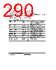
290 / 1504 page  Section 9 Bus Controller (BSC) Rev. 2.00 Sep. 24, 2008 Page 258 of 1468 REJ09B0412-0200 9.7.3 I/O Pins Used for Byte Control SRAM Interface Table 9.16 shows the pins used for the byte control SRAM interface. In the byte control SRAM interface, write strobe signals ( LHWR and LLWR) are output from the byte select strobes. The RD/ WR signal is used as a write enable signal. Table 9.16 I/O Pins for Byte Control SRAM Interface Pin When Byte Control SRAM is Specified Name I/O Function AS/AH AS Address strobe Output Strobe signal indicating that the address output on the address bus is valid when a basic bus interface space or byte control SRAM space is accessed CSn CSn Chip select Output Strobe signal indicating that area n is selected RD RD Read strobe Output Output enable for the SRAM when the byte control SRAM space is accessed RD/ WR RD/ WR Read/write Output Write enable signal for the SRAM when the byte control SRAM space is accessed LHWR/LUB LUB Lower-upper byte select Output Upper byte select when the 16-bit byte control SRAM space is accessed LLWR/LLB LLB Lower-lower byte select Output Lower byte select when the 16-bit byte control SRAM space is accessed WAIT WAIT Wait Input Wait request signal used when an external address space is accessed A23 to A0 A23 to A0 Address pin Output Address output pin D15 to D0 D15 to D0 Data pin Input/ output Data input/output pin |
|
リンク URL |
| ALLDATASHEETはお客様のビジネスに役立ちますか? [ DONATE ] |
Alldatasheetは | 広告 | お問い合わせ | プライバシーポリシー | データシートへのリンク | リンク交換 | メーカーリスト All Rights Reserved©Alldatasheet.com |
| Russian : Alldatasheetru.com | Korean : Alldatasheet.co.kr | Spanish : Alldatasheet.es | French : Alldatasheet.fr | Italian : Alldatasheetit.com Portuguese : Alldatasheetpt.com | Polish : Alldatasheet.pl | Vietnamese : Alldatasheet.vn Indian : Alldatasheet.in | Mexican : Alldatasheet.com.mx | British : Alldatasheet.co.uk | New Zealand : Alldatasheet.co.nz |
|
Family Site : ic2ic.com |
icmetro.com |
 Japanese ▼
 English
 Chinese
 German
 Japanese
 Russian
 Korean
 Spanish
 French
 Italian
 Portuguese
 Polish
 Vietnamese
 Indian
 Mexican
 British
 New Zealand